.png)

Action list:
In this lesson, we’ll review an MPPT project for solar panel applications, focusing on EMC (Electromagnetic Compatibility) and signal integrity. I’ll highlight some common mistakes that you’re likely to encounter more frequently when reviewing PCBs for low EMI. We’ll also explore techniques that can help improve the project’s performance in these areas.
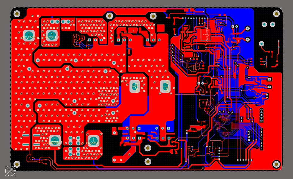
Stackup Analysis
When reviewing any project for EMI (Electromagnetic Interference), the first thing I would usually look at, is the board's stack-up. This is a key factor in the success of the project. The stack-up is particularly important because it affects around 90% of the project's EMC performance. Looking at the stack-up, we see it's a two-layer design. With signals placed on both the top and bottom layers, we can already anticipate potential issues. The main concern is the lack of a dedicated reference plane for the signal return paths, which can lead to EMC problems.
What Do We Mean by Return Reference Plane (RRP)?
A return reference plane (RRP) refers to a return plane that is adjacent to the signal traces. This is important because it provides the reference for the signal's voltage but also the path for the return current.
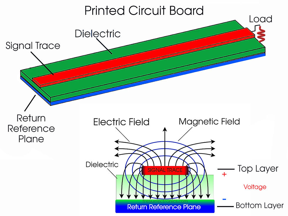
The reference plane also plays a major role in containing electromagnetic fields. Without it, the fields can spread out uncontrollably. In this project we are reviewing, there is no return reference plane underneath the signal traces, which will cause the fields to spread.
Another issue arises when there are two signal layers, such as signals on the top and bottom layers, as in this design. What happens here is that the fields from the top signal trace can interfere with the fields from the bottom signal trace, and vice versa.
This creates crosstalk, where signals from one trace are "seen" by the other trace. In simple terms, the fields from the top trace contaminate the fields of the bottom trace, and vice versa. When this happens, the signal on the top layer can affect the signal on the bottom layer, leading to unwanted interference.
Consider an example where you have a trace for a reset line and an adjacent trace for an interrupt signal. Let’s suppose you want to measure when the temperature rises above a certain level. The interrupt signal on the bottom trace is responsible for detecting this temperature rise. Meanwhile, the reset line on the top trace is used to reset your microcontroller or CPU.
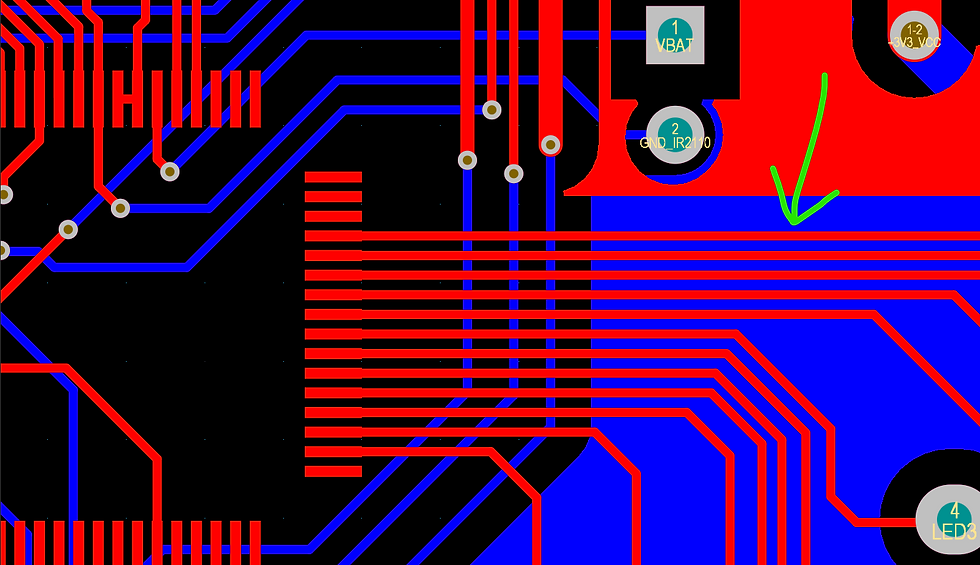
Here’s the issue: When the interrupt signal triggers, let’s say the temperature reaches 37°C, the CPU is supposed to take certain actions. The interrupt should notify the CPU to perform specific tasks. However, the reset signal, being on the top trace, also detects the high logic voltage level of the interrupt signal on the bottom trace. As a result, the CPU mistakenly interprets this as a reset request. Instead of responding to the interrupt, the CPU resets itself, because it thinks a reset has been triggered. This can lead to catastrophic failure, depending on the system and the actions required by the interrupt signal.
We want to ensure that the signal is contained within the dielectric in bewteen its conductor traces and that it is not contaminated by other signals. To achieve this, we need to ensure the fields are contained properly, which requires having a return reference plane that manages these fields.