Optimizing PCB Layout for EMI Control: Managing Fast-Changing Currents
- Dario Fresu

- Apr 4
- 7 min read
For electronic engineers responsible for designing printed circuit boards (PCBs), creating a functional layout requires more than just adhering to general guidelines; it necessitates a deep understanding of physics to effectively manage electromagnetic interference (EMI). This article delves into the essential principles of PCB layout, with a focus on managing rapidly changing currents (high di/dt) in power supply designs. By applying high school physics concepts such as the right-hand screw rule, Faraday’s Law, and Lenz’s Law, engineers can prioritize loop minimization, decrease inductance, and ensure EMC compliance in practical applications like buck converters.

The Challenge of PCB Layout Guidelines & EMI Control
The internet is filled with PCB layout advice—minimize loop areas, avoid jitter, reduce crosstalk—but these tips often lack detail or contradict each other. What does “as close as possible” to a component really mean? How far should “as far as possible” be from a noisy trace? In power supply designs, where rapidly changing currents are prevalent, such vagueness can result in less-than-ideal layouts. While all guidelines are valuable, their application depends on the context. Engineers must prioritize rules based on the circuit’s behavior, especially when dealing with currents that change rapidly (di/dt). This article addresses that gap by basing layout decisions on physics, providing a systematic method for handling high di/dt traces.
Physics Fundamentals: Magnetic Fields and Current Loops
Central to PCB layout is the understanding of currents and their related magnetic fields. The right-hand screw rule serves as a fundamental principle: when current passes through a conductor—like a PCB trace—a magnetic field is created around it. If you point your right thumb in the direction of the current, your fingers will curl in the direction of the magnetic field lines. Observed from above, a current moving toward you (usually depicted by a dot) creates clockwise field lines, while a current moving away from you (typically shown as a cross) produces counterclockwise fields.
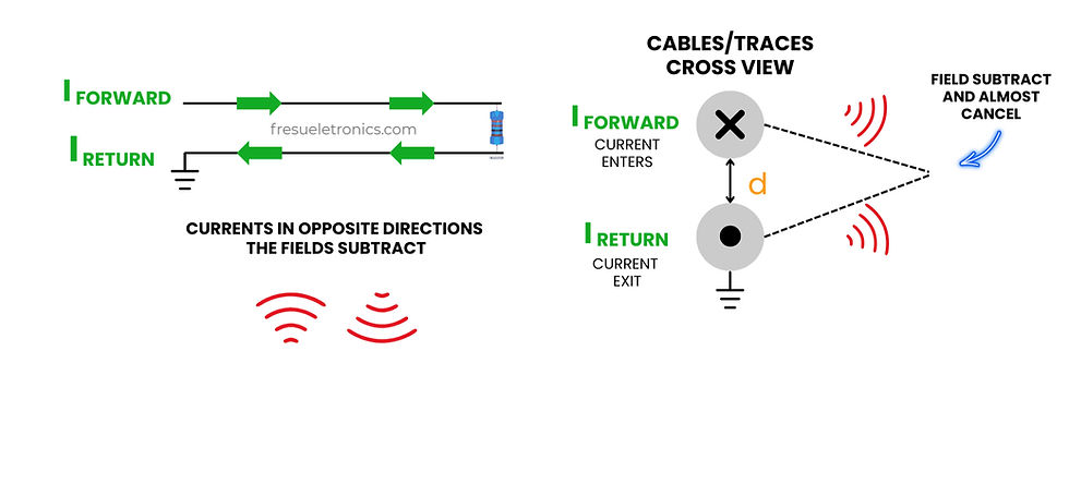
In practical circuits, currents travel in loops rather than endlessly, as in theoretical models. A forward current originating from a source must return to it, creating a closed circuit. The loop's size and orientation determine the magnetic field's intensity and extent. A larger loop area enhances the field, raising inductance and EMI, whereas a smaller loop diminishes both. Additionally, if the forward and return paths are arranged to generate opposing magnetic fields, they can neutralize each other outside the loop, reducing interference—an essential principle for designing quiet PCBs.
Loop Area and Inductance: A Practical Perspective
Consider a PCB with a current loop viewed from the side. A forward trace carries current away, while a return trace brings it back. Using the right-hand screw rule, the magnetic fields inside the loop reinforce each other, proportional to the loop area, similar to a single-turn inductor. Outside the loop, if the traces are far apart, the fields remain distinct and uncanceled, leading to EMI radiation. By reducing the loop area and routing the return path closer to the forward path, the inductance decreases. Even better, if the currents are equal and opposite (a mirror pair), the external fields cancel out, keeping the PCB "quiet" beyond the traces. This dual advantage—lower inductance and field cancellation—makes minimizing the loop a fundamental aspect of EMC compliance.

The most efficient approach for minimizing electromagnetic interference (EMI) is to arrange the forward and return current paths vertically across the layers of a PCB. On a two-layer board, positioning the return path directly beneath the forward trace confines the magnetic field within the board’s dielectric material, reducing the loop area and mitigating external EMI through effective field cancellation. When the return current flows to circuit reference ground via a solid and unbroken plane on an adjacent layer, physics ensures it follows the path of least inductance—typically directly under the forward trace at high frequencies. This natural alignment enhances cancellation of the magnetic fields without requiring manual routing of the return path, making it an elegant and automatic solution for improving signal integrity and reducing EMI.
AC vs. DC: Prioritizing High di/dt Traces
Not all currents demand equal attention in PCB design. DC currents generate static magnetic fields, with field lines encircling the current loop much like those of a permanent magnet. These fields remain constant and do not induce voltages in nearby traces unless they change, making DC loops less critical to minimize for EMI purposes. In contrast, AC or time-varying currents produce dynamic magnetic fields that fluctuate with the current. According to Faraday’s Law, the induced electromotive force (EMF) in a nearby conductor is proportional to the rate of change of magnetic flux (dΦ/dt), which scales with the current’s di/dt. A higher di/dt—common in high-frequency signals or fast transients—amplifies the induced voltages, elevating EMI risks and necessitating careful loop minimization to protect signal integrity.
For a trace with self-inductance L, the induced voltage across it is V = -L di/dt. For mutual inductance M between traces, the voltage induced in a nearby trace is V = -M di/dt. Imagine a 10 cm long, 0.5 mm wide trace on a PCB, like one carrying power to an LED that blinks on and off. Suppose it has an estimated inductance of 10 nH/cm (totaling 100 nH). If the LED current switches from 0 to 2 A in 50 ns (di/dt = 40 x 10^6 A/s), it creates a 4 V spike across itself. Now, picture a nearby trace—say, one connected to a microcontroller’s reset pin—with 2 nH of mutual inductance. This trace picks up a 0.08 V spike. While that seems small, it’s enough to glitch a reset pin, which might only tolerate 0.05 V of noise before resetting the microcontroller by mistake. This shows why traces with fast-changing currents, like those in blinking LEDs or power circuits, need small loops to lower inductance and must be kept away from sensitive signals to avoid EMI trouble.
High-Frequency Behavior: Path of Least Inductance
In DC circuits, current follows the path of least resistance, which can spread out across a return and reference plane ("ground") and sometimes form larger loops depending on the layout. At high frequencies, current takes the path of least inductance, naturally flowing directly beneath the forward trace in a ground plane to minimize loop area and EMI. This alignment happens automatically due to the physics of inductance, which twisting conductors or stacking them vertically can mimic—reducing loop area and canceling magnetic fields. In a solid return and reference ("ground") plane, high-frequency return currents stay under the source trace, lowering EMI without extra routing, as long as no cuts or slots lie beneath traces with high di/dt. Cuts under DC paths are not as problematic, but under switching traces, they force return currents to detour, increasing loop area and EMI risks.
Applying Principles to a Buck Converter
Switching power supplies, such as buck converters, present significant high di/dt challenges. The critical loops include the switch path (MOSFET), diode path, inductor ripple, capacitor ripple, and DC output. When the MOSFET is activated, current travels from the input through the MOSFET and inductor, supplying the load (DC) and charging the capacitor (AC), before returning to the input. When the MOSFET is deactivated, the diode maintains the inductor current, forming a loop through the diode, inductor, and load/capacitor. The current waveforms in a buck converter display distinct characteristics. The switch (MOSFET) and diode currents quickly turn on and off, exhibiting sharp transitions that occur in tens of nanoseconds (high di/dt). The inductor and capacitor currents fluctuate steadily, creating a ripple effect during the switching cycle (moderate di/dt). The load current remains flat and constant, resembling a straight line (no di/dt).
Prioritization is simple: the switch and diode loops are the primary sources of EMI due to their rapid transitions. The switch current can be aligned with its return path for cancellation by routing them closely together, but the diode loop's return is less straightforward, making it more challenging to control. Inductor and capacitor ripple loops are less critical, and DC loops have minimal impact on EMI. Following a schematic linearly results in extensive loops that increase EMI. Instead, arrange components in a U-shape, positioning input and output connectors near each other to minimize the switch and diode loops. A ground plane on the bottom layer aids by directing return currents under the high di/dt traces for cancellation—just ensure that these paths are uninterrupted. DC paths can accommodate cuts, but switching paths cannot.

Control Circuitry and Sensitive Signals
In switching power supplies, control circuitry requires careful consideration beyond just the power paths. The gate drive signal to the MOSFET, which has a fast-switching current (high di/dt), should have a compact loop between the control IC and the switch to reduce inductance. For voltage-mode control, the feedback voltage from a voltage divider is susceptible to noise, so it should be placed close to the IC rather than the output to shorten traces and avoid high-di/dt areas like the switch node. In current-mode control, the signal from the current sense resistor is crucial and sensitive, so it should be positioned near the IC for accuracy. Grounding is essential: connect the signal and power grounds together, and do not separate them as some application notes suggest.
Precision Layout for EMC Success
Effective PCB layout relies on the application of physics to control rapidly changing currents. Engineers can manage EMI in power supply designs, such as buck converters, by minimizing high di/dt loops, using reference ground planes for cancellation, and isolating sensitive signals. Priority should be given to the switch and diode paths, followed by ripple currents, with DC loops being less critical. Strategic placement of components and multilayer routing can convert complex schematics into EMC-compliant boards. For electronic engineers, these principles, grounded in high school physics, provide a clear and practical approach to creating robust, quiet PCB designs that meet performance and regulatory standards. If you're eager to dive deeper into EMI control, we invite you to explore our engaging online course or EMI Control Guides. Discover a wealth of knowledge and practical skills that will empower you to take your understanding to the next level.


Opmerkingen