

Mastering Electromagnetic Interference: Elevate Electronics with EMC Design
- Dario Fresu

- Apr 23
- 7 min read
Updated: May 25

Introduction
Electromagnetic compatibility (EMC) is a critical aspect of electronics design, ensuring that devices operate reliably without causing or succumbing to electromagnetic interference (EMI). As circuits become denser and operate at higher speeds, achieving EMC becomes increasingly challenging. Inadequate EMC design can result in signal degradation, regulatory non-compliance, and extensive redesign efforts, compromising product performance. Conversely, efficient EMC design enhances functionality, streamlines development, and improves reliability.
The foundation of efficient EMC design lies in the laws of physics, particularly Maxwell’s equations and Faraday’s law, which govern all electrical activity. By aligning circuit design with these principles, engineers can create systems that naturally minimize EMI, optimize signal integrity, and enhance performance. This article explores how to achieve efficient EMC design through physics-based principles, focusing on minimizing current loop areas, implementing low-impedance reference planes, and applying strategic decoupling and filtering. It also addresses common misconceptions that hinder EMC performance, providing a clear framework for designing electronics that excel in both laboratory testing and real-world applications.
Mitigating Electromagnetic Interference
Electromagnetic compatibility ensures that electronic devices function as intended within their electromagnetic environment, neither emitting excessive interference nor failing under external EMI. EMC encompasses two primary domains:
Internal EMC: This focuses on signal integrity within a circuit, addressing issues such as crosstalk, jitter, ringing, and signal-to-noise ratio degradation. Internal EMC directly influences a device’s functional reliability, such as the accuracy of analog signals or the stability of digital data.
External EMC: This involves meeting regulatory standards, such as the EMC Directive, and ensuring robust performance in diverse electromagnetic environments. External EMC prevents interference with other devices and maintains device reliability, enhancing user satisfaction and reducing maintenance issues.
Achieving EMC requires balancing these requirements while optimizing development time and resources. Traditional design approaches often rely on iterative testing or outdated methods, leading to delays and inefficiencies. A physics-based approach, rooted in the fundamental behavior of electromagnetic waves, enables engineers to design circuits that inherently perform well, reducing the need for extensive revisions.
The Physics of EMC: Electromagnetic Waves and Current Flow
All electrical activity in electronics—whether power, signals, or noise—propagates as electromagnetic waves, governed by Maxwell’s equations. These equations describe the interplay of electric and magnetic fields, influenced by the properties of the medium:
Permeability (μ): Associated with magnetic fields and inductive energy, permeability determines a medium’s ability to support magnetic flux.
Permittivity (ε): Linked to electric fields and capacitive energy, permittivity governs the storage of electric charge.
The velocity of an electromagnetic wave is defined by the equation
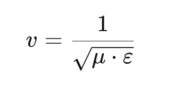
In air or a vacuum, this velocity approaches the speed of light (approximately 300 million meters per second), and the wave impedance is approximately 377 ohms

In media such as PCB fiberglass or cable insulation, higher permittivity reduces both velocity and impedance, affecting current flow paths.
Faraday’s law of electromagnetic induction provides a key principle for EMC design:
Currents seek loops with the smallest area, as these have the lowest impedance.
Impedance, comprising resistance, inductance, and capacitance, varies with frequency. At low frequencies, resistance dominates, but at higher frequencies, inductance becomes more significant, driving currents toward paths that minimize loop area. Small loop areas produce compact electric and magnetic field patterns, reducing emissions and susceptibility to external interference.
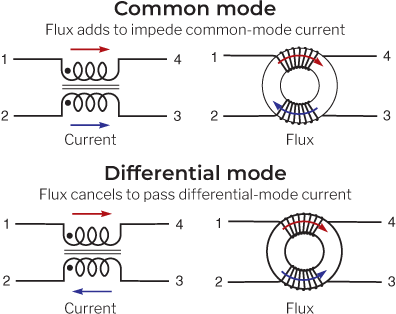
Currents in electronics are classified into two types:
Differential-mode currents: These are intended currents flowing in designed loops, such as signal or power paths, producing smaller field patterns and causing minimal EMI.
Common-mode currents: These are unintended currents, often arising from impedance discontinuities, stray capacitance or circuit imbalances, flowing in larger loops, such as between a circuit and a chassis. Common-mode currents are the primary source of EMI due to their larger loop areas, which act as efficient antennas.
By understanding these principles, engineers can design circuits that align with the natural behavior of electromagnetic waves, minimizing interference and optimizing performance.

Conductors as Accidental Antennas
Every conductor in a circuit acts as an accidental antenna, capable of radiating or receiving electromagnetic energy. The effectiveness of this antenna effect depends on the loop area of the current path. Larger loops have higher impedance and generate broader field patterns, increasing both emissions and susceptibility to external EMI. This behavior is governed by the principle of reciprocity:
A conductor that radiates energy at a specific frequency is equally susceptible to interference at that frequency.
Resonances pose a significant challenge in EMC design. They occur when inductive and capacitive impedances are equal or when a conductor’s geometry aligns with a signal’s wavelength, creating standing waves. At resonant frequencies, loop impedances can fluctuate dramatically—from milliohms to megaohms—amplifying emissions or susceptibility by up to 100 times. Efficient EMC design minimizes loop areas and mitigates resonances, ensuring compact field patterns and stable performance across a wide frequency range.
Common Misconceptions in EMC Design
Several misconceptions in EMC design lead to suboptimal performance and inefficiencies. Addressing these is critical for adopting a physics-based approach.
Misconception 1: Grounding Eliminates Noise
A prevalent belief is that connecting a circuit to a safety (earth) ground removes unwanted noise currents. In reality, all conductors, including ground connections, have impedance, and currents flow in closed loops. Grounding is primarily a safety measure to protect against electrical faults, not a solution for EMC. Ground structures, such as chassis or bonding networks, serve as return paths for currents, not as infinite sinks for noise. Designing with the assumption that grounding eliminates EMI often results in uncontrolled common-mode currents and increased interference.
Misconception 2: Split Ground Planes Control RF Currents
Another misconception is that splitting ground planes on a PCB confines radio frequency (RF) currents to specific areas, reducing crosstalk between sections like analog and digital circuits. However, RF currents can travel through air, stray capacitances, or other unintended paths, bypassing splits and causing noise. Split ground planes increase impedance, disrupting the low-impedance return paths essential for EMC. This practice has been recognized as ineffective since the rise of high-speed microprocessors, yet it persists in some designs.
Misconception 3: Minimizing Component Costs Ensures Efficiency
Many engineers focus on minimizing the Bill of Materials (BOM) cost, assuming it drives design efficiency. While reducing component costs is important, poor EMC design leads to multiple redesigns, delayed development, and increased maintenance expenses, undermining overall efficiency. Efficient EMC design, even if it requires additional components like capacitors or filters, streamlines development, enhances reliability, and optimizes long-term performance, making it a more effective strategy.
Practical EMC Design Principles
To achieve efficient EMC design, engineers can apply three physics-based principles that align with the natural behavior of electromagnetic waves. These principles minimize EMI, enhance signal integrity, and streamline development.
Principle 1: Minimize Current Loop Areas
The first principle is to design circuits with the smallest possible current loop areas. By positioning forward and return conductors—such as signal traces and their "ground" returns—close together, engineers can reduce loop area, lowering impedance and producing compact field patterns. For instance, routing a signal trace directly above a continuous return and reference plane (RRP) on a PCB minimizes the loop area compared to routing it far from its return path. Smaller loops reduce electromagnetic coupling with other circuits, decreasing crosstalk, emissions, and susceptibility to external interference.
Principle 2: Implement a Continuous Return & Reference Plane
A continuous, low-impedance return & reference plane, typically called a solid ground plane, is crucial for efficient EMC. This plane should span the entire PCB, extending beyond all traces and components, to provide a preferred path for return currents. Unlike split ground planes, a continuous return reference plane maintains low impedance across a wide frequency range, confining both differential-mode and common-mode currents. For safety-critical applications, such as power supplies, isolation barriers may necessitate limited splits, but these should be minimized to avoid disrupting current paths.
Principle 3: Use Strategic Decoupling and Filtering
Decoupling and filtering are essential for controlling currents and preventing EMI. Decoupling involves placing capacitors near devices to create low-impedance paths for differential-mode currents in DC power rails, forming small, localized loops that prevent currents from spreading across the PCB and generating noise. Filtering addresses common-mode currents by installing components, such as capacitors, resistors, or ferrites, at points where traces connect to off-board conductors, like I/O cables or power lines. These filters bond conductors to the RF reference plane, providing a low-impedance path for common-mode currents and preventing them from radiating through cables, which act as accidental antennas.
Applying EMC Principles in Practice
Imagine a scenario where you are designing a microcontroller-based device. To ensure EMC, You apply the three principles:
Loop Area Minimization: Signal traces are routed close to their "ground" (return and reference) plane, reducing loop areas and minimizing crosstalk between digital and analog sections.
Continuous Return & Reference Plane: A solid return and reference plane is implemented across the PCB, providing a low-impedance path for return currents and eliminating splits that could increase noise.
Decoupling and Filtering: Decoupling capacitors are placed near each integrated circuit to reduce trace inductance and localize differential-mode currents. Filters are added at each cable entry points to suppress common-mode currents.
These measures ensure the device meets regulatory standards, performs reliably in diverse environments, and requires fewer design iterations, enhancing overall efficiency.
Benefits of Physics-Based EMC Design
Adopting a physics-based approach to EMC design offers several advantages:
Enhanced Signal Integrity: Small loop areas and low-impedance paths improve signal-to-noise ratios and reduce crosstalk, ensuring reliable operation.
Reduced Emissions and Improved Immunity: Compact field patterns minimize radiated EMI and susceptibility to external interference, simplifying compliance testing.
Streamlined Development: Aligning with electromagnetic principles from the start reduces the need for redesigns, accelerating development cycles.
Improved Reliability: Robust EMC design ensures consistent performance in real-world conditions, enhancing user satisfaction, and fewer product returns.
Resource Optimization: Faster development and greater reliability outweigh the modest cost of additional components like capacitors or filters.
Conclusion
Efficient EMC design is rooted in the fundamental laws of physics, leveraging Maxwell’s equations and Faraday’s law to create electronics that excel in performance and reliability. By understanding electrical activity as propagating electromagnetic waves, engineers can design circuits that naturally minimize interference. The principles of minimizing loop areas, implementing continuous RF reference planes, and using strategic decoupling and filtering provide a clear framework for success. Dispelling misconceptions about grounding, split planes, and cost priorities empowers engineers to make informed decisions.
As electronics advance with higher speeds and greater integration, the importance of EMC design will continue to grow. At Fresu Electronics, we are dedicated to helping engineers grasp and implement best design practices from the outset. If you're interested in enhancing your skills, we invite you to explore our courses and EMI control guides.


Comments