.png)

Action list:
In this lesson we dive deep into the review of the iMX8 processor PCB, focusing on Electromagnetic Compatibility (EMC) and signal integrity.
We start by analyzing the stack-up of the board, identifying potential issues with mixed signal layers, power planes, and return reference planes. Throughout the lesson, we will highlight specific problem areas, and provides recommendations to enhance board design for better EMC compliance and signal integrity.
Stackup analysis
The first aspect to examine is the board's stack-up. Understanding the stack-up is essential to evaluate how the fields will behave in this system on module. Analyzing the stack-up reveals several key details, starting with the fact that it consists of the following layers:
Layer 1 - Mixed Signals
Layer 2 - Power Plane
Layer 3 - Power Plane
Layer 4 - Signals
Layer 5 - Signals
Layer 6 - Mixed Signals

At first glance, there could be potential issues. A mixed signal layer means that both signals and power are integrated on the same layer. Directly beneath it is a power plane, which ideally should be a return reference plane (RRP). However, what catches the attention is the additional plane on layer three. This plane could potentially be another power plane, but there’s uncertainty around its exact role.
🔓 Ideally, we want to ensure that each signal and power layers are paired with their respective return reference plane (RRP).
This principle is crucial for maintaining signal integrity and preventing electromagnetic interference (EMI). Replacing a return reference plane with another signal layer to reduce costs might seem appealing, but this approach often backfires. While it may appear to save money by eliminating a layer, the actual costs become evident during EMC tests or signal integrity checks.
🔓 It is important to remember that a signal voltage is defined by two potentials: the signal's active potential and its reference potential.
If one of these potentials is removed, we’re left with only one potential, which means there’s no longer a voltage difference to define the signal.
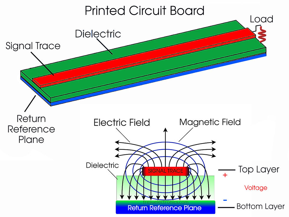
Without both potentials, a usable signal may not exist, or any signal present will likely rely on parasitic elements. These parasitics can provide a return path to close the current loop, but this compromises signal quality. When selecting a stack-up, it is essential to think in terms of pairs.
🔓 Signal (and power) layers should always be paired with their corresponding return reference planes.
This pairing forms the foundation of effective stack-up design and helps prevent issues with signal integrity and electromagnetic compatibility.
Digital signal layers should always be placed adjacent to a return or reference plane. Without a reference plane, a single signal layer effectively functions like an RF board, promoting signal emission rather than supporting digital or mixed-signal designs. This approach can lead to significant electromagnetic compatibility issues and should be avoided. When a return reference plane is absent next to the signal, significant radiation can be emitted. This concept is explained in greater detail in the 'Radiated Emissions' lesson available in the courses and blog.
From a manufacturing perspective, the stack-up should be designed as a mirror image, with one side of the board reflecting the other. For a six-layer board, as in this case, if a return reference plane is placed on the second layer, another return reference plane should be placed on the fifth layer. This principle of symmetry applies to other layers as well. Such symmetry is essential to ensure consistent and predictable electrical and mechanical behavior of the board.
A symmetrical stack-up is particularly important for the board's thermal behavior. An asymmetrical stack-up can cause uneven heating, leading to warping. This warping may place stress on solder joints, potentially causing components to detach from the board. Such mechanical failures could be easily avoided with a well-designed stack-up.
To prevent these issues, it is essential to aim for a symmetrical stack-up. Pair each signal layer with a return reference plane and strive to make the overall stack-up as balanced as possible. A symmetrical design enhances not only electrical performance but also the mechanical integrity of the board, ensuring greater reliability and robustness over time.