.png)
Fundamentals of PCB Design For EMC & Low EMI
- Dario Fresu

- Nov 13, 2024
- 9 min read
Updated: Feb 24
CLICK THE PLAY BUTTON TO WATCH THE LESSON.
Action list:
In this article, we are going to explore the fundamental concepts necessary to understand Printed Circuit Board design for passing EMC.
In electronics or electrical circuits classes, we have learned to design circuits according to the water through the pipes analogy. Although those analogies are helpful for simplifying circuit design, when we discuss printed circuit board design, we have to take one step back and consider the true fundamentals, the Maxwell's equations.

Before you decide to run away from this lesson, what we need at this point as designers is not so much to go back and understand the math of the equations, but rather to understand the principles behind them, in this way, we can visualize these effects and build boards that excel in terms of reliability, immunity to disturbances, and compatibility with other systems.
🔓 This means that we ensure that our system can work with other nearby devices and systems, without disrupting its normal operation, or the normal operation of other devices.
To be able to do that, we need to visualize the electromagnetic fields in a printed circuit board trace, at least at a basic level. Let's now take a simple example of a printed circuit board and analyze how it can helps us visualize the fields. In this picture, we can see a cross section view of a double layer printed circuit board.
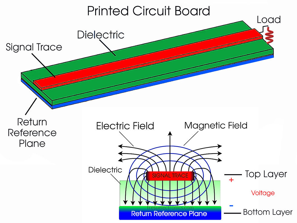
The top layer is represented by the red colored signal trace, and the bottom trace for the reference plane is represented by the blue color. Also, to complete the picture, we have the dielectric layer (in green), which is placed between the signal layer on the top, and the return reference plane on the bottom layer.
From this picture, we can observe that different phenomena are occurring. The first thing we notice is the presence of fields. The electric field described from the black arrows and the magnetic field described by the blue circles. Of course, this assumes that a signal is present on the signal trace. Here, we can observe that the electric field lines are radiating from the signal trace.

Their direction changes depending on the position of the trace in relation to the return reference plane. In this PCB, where the return reference plane is close to a signal trace, the electric fields generated by the signal trace are naturally drawn towards this plane and terminate there. On the top side of the signal trace instead, where there is no return reference plane, the electric field lines from the signal trace are partially uncontained.
Why is this important for us?
Without a return reference plane (RRP) close to the signal trace, electric fields can extend further, grow larger, and may interact with unintended parts of the circuit, or external environments, potentially leading to electromagnetic interference issues. This is why return reference planes are critical in PCB design, to ensure controlled propagation of electric and magnetic fields and to minimize interference.
Many of the problems we encounter during EMC tests, in fact, arise from poorly designed layouts where the fields are not well contained and extend further disrupting the operation of other devices or components.
🔓 If you think about it, during EMC tests such as radiated and conducted tests, what we are measuring is the energy level of these fields.
The quickest way to encounter EMC issues, in fact, is to remove the return reference plane from the vicinity of the signal trace. This allows the fields to expand and create disruptions in undesired locations. In simple terms, when this is done, the electric fields are no longer confined and can grow larger, possibly reaching other devices or component structures. When this occurs, the return current loops, formed through parasitic paths, will also grow, causing an increase in electromagnetic fields that can further disrupt operations.
Want to read more?
Subscribe to fresuelectronics.com to keep reading this exclusive post.